
High Speed Design
Practical Timing Analysis for 100-MHz Digital Designs
By Bob Kirstein, Stratus Engineering
MOST TECHNICAL LITERATURE ON HIGH-SPEED DESIGN FOCUSES ON TERMINATION, RINGING, AND CROSSTALK. DESPITE SIGNAL INTEGRITY’S IMPORTANCE, INADEQUATE TIMING MARGINS CAUSE MANY MORE ERRORS IN TODAY’S 100-MHz DIGITAL DESIGNS.
As increasing chip complexity, high clock rates, and analog signal-integrity issues complicate digital design, time-to-market pressures continue to shorten development schedules. These factors present increasing challenges to digital-design engineers, who must spend more time understanding software and system-level issues and have less time for details such as timing analysis. Because you can’t ignore board-level propagation delays in today’s more-than-100-MHz designs, detailed timing analysis is essential.
This analysis develops general timing-margin equations, which include the effects of clock skew and propagation delay. A fast and effective procedure for analyzing timing margins uses a spreadsheet instead of traditional timing diagrams. This approach quickly identifies approximate timing margins early in the design. A little extra work can improve the margins, reduce the parts cost, or reduce engineering or pc-board-layout effort.
DIGITAL-TIMING REVIEW
A good starting point is a review of the timing requirements for a typical synchronous digital connection, such as the one in Figure 1.
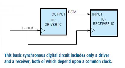
In this circuit, the driver, IC1, produces valid data after a delay of TCO from the rising clock edge. The data must arrive at IC2 in time to meet the receiver’s input setup-and-hold-time requirements.
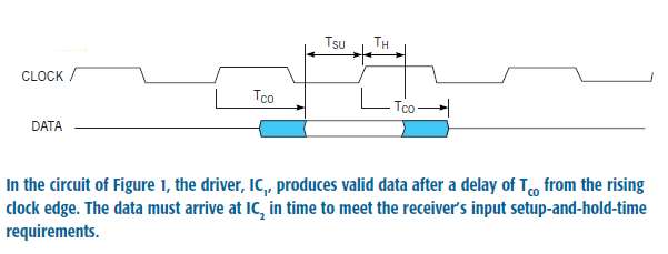
MINIMUM CLOCK PERIOD=TCO(MAX)+TSU ,
SETUP MARGIN=CLOCK PERIOD-TCO(MAX)-TSU ,
and
HOLD MARGIN=TCO(MIN)-TH ,
where TCO(MIN) and TCO(MAX) are the manufacturer specified minimum and maximum clock-to-output propagation-delay values for IC1‘s output, and TSU and TH are the manufacturer-specified minimum setup-and-hold times for IC2‘s input. Note that although you can always increase the clock period to increase the setup margin, increasing the clock period does not affect the hold margin, leading to the following important result: Input-hold margin is independent of clock frequency.
This result indicates the importance of verifying hold-time requirements during a project’s design phase, because you can’t eliminate hold-time violations by simply lowering the clock frequency.
BOARD-LEVEL PROPAGATION DELAY
The simple example of Figure 1 neglects data propagation delay and clock skew between the transmitting and receiving ICs. In real digital systems in which clock signals reach frequencies of 100 MHz and higher, board-level-propagation or TOF (time-of-flight) delays are significant. In fact, at these high speeds, controlling clock skew is often necessary for producing adequate timing margins. To perform a realistic timing analysis, you must therefore modify the basic timing model to include clock skew and propagation delay. To model TOF and clock skew, the diagram in Figure 3 introduces separate signals for clock and data at the driver and receiver.
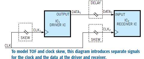
In this diagram, CLK1 and DATA1 represent signals at the driver, and CLK2 and DATA2 represent signals at the receiver.
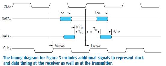
SETUP MARGIN= CLOCK PERIOD-TCO(MAX)-TSU– TOFD-TSKEWC , (1)
HOLD MARGIN=TCO(MIN)-TH+ TOFDTSKEWC , and (2)
MINIMUM CLOCK PERIOD= TCO(MAX)-TCO(MIN)+TSU+TH ,
where TOFD is the propagation delay, or TOF for the data path between IC1 and IC2. TSKEWC is the clock skew from IC1 and IC2, defined as positive when IC2 is clocked later in time than IC1. You can establish a lower bound on the clock period by setting the setup-and-hold margins to 0 in equations 1 and 2, yielding:
CLOCK PERIOD.TCO(MAX)+TSU+ (3)
TOFD-TSKEWC ,
and
TCO(MIN)=TH=TOFD+TSKEWC , (4)
Eliminating the term (TSKEWC-TOFD) by substitution in equations 3 and 4 leaves you with the following relationship for minimum clock period:
MINIMUM CLOCK PERIOD= TCO(MAX)-TCO(MIN)+TSU+TH .
This equation indicates that if you can control clock skew, the maximum achievable clock frequency for this circuit is independent of propagation delay, leading to the following important result: For unidirectional signaling, the uncertainty in driver propagation delay and the receiver setup-and-hold times limit the clock frequency, but the clock frequency is independent of the overall propagation-delay magnitude.
POSITIVE SKEW
In this example, the clock skew is positive, which means that IC2 is clocked after IC1. In general, TSKEWC can be either positive or negative. As you will see, the ability to adjust TSKEW provides considerable flexibility in optimizing timing margins. With this timing model, you can introduce delays to the clock signals, the data signals, or both to improve timing margins, thereby increasing clock frequency.
You can make the several important observations in conjunction with this timing model. Delaying the clock signal by increasing the pc-board clock-trace length relative to the data-trace length increases the setup margin at the expense of the hold margin, allowing the circuit to operate at a higher frequency. Delaying the data signal by increasing the pc board data-trace length relative to the clock-trace length increases hold margin at the expense of setup margin. Additional hold margin may be necessary to accommodate devices with unusually long hold times. When TSKEWC is equal to TOFD, the clock skew exactly compensates for TOF, and equations 1 and 2 give the same results as the previous model, which ignores TOF. For this example, which models the special case of unidirectional signaling, you can usually use a very fast clock, regardless of the propagation delay, as long as the data and clock delays are equal. In this case, (TCO(MAX)-TCO(MIN)) rather than |TCO| (the magnitude of TCO) limits the clock frequency.
As you will see, you can’t draw the same conclusion in the case of bidirectional signaling. In many cases, an IC with less TCO uncertainty is easier to use in a high-speed design than one with a smaller overall TCO. For this reason, IC manufacturers should always specify accurate TCO(MIN) values. As an example, consider a design that interfaces a device with 0 or unspecified TCO(MIN) to an SDRAM with a 1-nsec input-hold-time requirement. Whereas the SDRAM’s TCO(MIN) is unlikely to ever be less then 1 nsec, strictly meeting the 1-nsec SDRAM hold time requires that you add 1 nsec (about 6 in.) of board-trace delay, thereby sacrificing 1 nsec of setup margin.
GENERALIZED TIMING MODEL
Because most digital connections involve inputs as well as outputs on each IC, the next step is to extend the timing model to include bidirectional signaling.
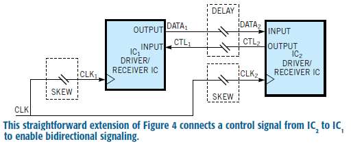

IC2 SETUP MARGIN= CLOCK PERIOD-TCOU1(MAX)– TSUU2-TOF+TSKEWC;
IC2 HOLD MARGIN=TCOU1(MIN)– THU2+TOF-TSKEWC;
IC1 SETUP MARGIN= CLOCK PERIOD-TCOU2(MAX)– TSUU1-TOF-TSKEWC;
and
IC1 HOLD MARGIN=TCOU2(MIN)– THU1+TOF+TSKEWC.
The timing diagram in Figure 6 is too complicated for everyday use. Moreover, there is no longer a closed expression for minimum clock period because there are too many parameters. Fortunately, you can easily perform timing analysis for this model with a spreadsheet. Before beginning the spreadsheet analysis, observe the following about the bidirectional-signaling model:
- Delaying the clock signal to IC2 by increasing the pc-board clock-trace length increases data-setup margin at IC2 and increases CTL-hold margin at IC1 at the expense of decreased data-hold margin at IC2 and decreased CTL-setup margin at IC1.
- Delaying the clock signal to IC1 by increasing the pc-board clock-trace length increases CTL-setup margin at IC1 and increases data-hold margin at IC2 at the expense of decreased CTL-hold margin at IC1 and decreased data-setup margin at IC2.
- Increasing the TOF for a signal increases its hold-time margin at the expense of setup margin.
In general, when both devices’ TCO, TSU, and TH specifications are the same, setting TSKEWC to 0 yields optimal timing margins.
When the devices have different timing requirements, you can usually introduce clock skew to improve the timing margins. Note also that when the TCO(MIN) and TOF are both small, meeting input-hold-time requirements can be difficult. This observation suggests that closer is not necessarily better from a timing standpoint. In any case, when timing margins are tight, you should always do a detailed analysis to verify timing and to establish detailed layout instructions.
ESTIMATING TIME OF FLIGHT
To determine and optimize timing margins, you need a reliable method for estimating TOF. Initially apply this method to estimate preliminary timing margins from parts-placement data and then later to create pc-board-layout instructions. The two primary components in TOF are propagation delay in the pcboard traces and capacitive-loading delay. Trace delay varies only slightly because of variations in the pc-board dielectric and characteristic impedance.
You can usually get results accurate to within about 10% by multiplying 170 psec/in. (about 6 in./nsec) by the trace length in inches. Accuracy is important, because you use trace length to control clock skew and TOF delay when you optimize timing margins.
Capacitive loading, however, wreaks havoc in designs by causing waveform distortion and introducing delays that depend on bus topology and driver characteristics. Loading delays are less predictable than propagation delays because of variations in capacitance, but these delays always increase TOF, leading to another important point: TOF delays caused by capacitive loading always decrease setup margin and increase hold margin.
In TOF calculations, don’t combine loading delays with propagation delays; estimate them separately and then provide sufficient setup margin in the final design to compensate for the delays. For complicated bus structures that have multiple loads and tight timing margins or when driving SDRAMs and DIMMs, a transmission-line simulator is the best way to ensure accurate TOF calculations. However, for simple bus structures with light loads, you can simply allow 50 psec of additional setup margin for each picofarad of load capacitance. The following analysis uses this rule of thumb and defers detailed TOF calculations.
SPREADSHEET ANALYSIS
You now have a model that you can use to perform detailed timing analyses on most high-speed digital designs, but the associated timing diagrams are confusing, and creating them is time-consuming. The equations for timing margins can save a lot of time because you can use them in a spreadsheet analysis, such as the one in Table 1.
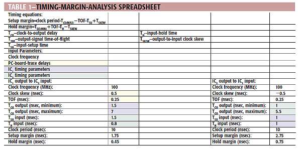
Using this spreadsheet, enter the manufacturer’s timing parameters, estimate TOF using preliminary placement data, and then adjust the clock skew to optimize the timing margins. You can summarize the spreadsheet design procedure as follows:
1. Enter the clock frequency and each device’s manufacturer-specified values of TCO(MIN), TCO(MAX) , TSU, and TH .
2. Using the preliminary parts-placement and pc-board-constraint data, estimate the trace length and TOF for the signals of interest. Enter the TOF into the spreadsheet.
3. Adjust the clock skew (and possibly the TOF) to optimize the timing margins for both devices.
4. Create pc-board-layout instructions to implement the required clock skew and TOF delays.
The values in this spreadsheet example come from a design that uses a Texas Instruments TMS320C6211 DSP with PC100 SDRAM operating at 100 MHz. For this design, the microprocessor is close to the SDRAM, so you can use a minimum value of 0.25 nsec for TOF, which corresponds to a minimum trace length of about 1.5 in. Because capacitive loading increases the hold margin and decreases the setup margin, the strategy is to maximize the setup margin and then estimate the additional capacitive loading and trace delay that the design supports. Ideally, you want enough margin to use an automatic router on the SDRAM-data and -control signals.
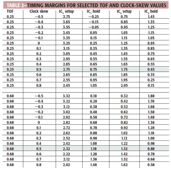
Suppose that instead of requiring the pc-board designer to match data- and control-signal lengths (a time-consuming task), you constrain these lengths to fall between 1.5 and 4 in. (You might expect this type of variation in trace length from the output of an automatic routing program.) To analyze the timing for these constraints, you can examine the worstcase margins for the longest and shortest traces with various values of clock skew. You can then choose a clock skew that gives acceptable overall margins.
CLOCK SKEW AND TOF
After determining timing margins and the required implementation delays, your next task is to design the clock architecture and create pc-board-layout instructions. In general, the best way to make clock-skew and TOF adjustments is to control the length of the associated signal traces during pc-board layout. Controlling trace lengths is a painful task for pc-board designers. In addition, one of the primary design goals is to minimize pc-board-layout constraints. Careful planning during parts placement is particularly important to achieving this goal.
Figure 7 shows the clock architecture for a typical 100-MHz-microprocessor SDRAM interface. The microprocessor supplies a bus clock, which serves as the timing reference for all data and control signals. A PLL clock driver distributes this clock to the SDRAMs and other peripherals. In this architecture, the PLL contains an external feedback path, which is the key to controlling clock skew between the microprocessor and its peripherals.
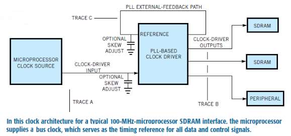
The PLL clock driver’s output clocks advance in time by an amount equal to the feedback-path trace delay. You can compensate for the propagation delay from the microprocessor to the peripherals to achieve zero clock skew, or you can introduce positive or negative clock skew by controlling the length of traces A, B, and C as follows:
Case 1: C=A+B; skew=0. In Case 1, the feedback path exactly compensates for the clock delay from the microprocessor to the peripherals. The clock driver’s outputs advance so that the clock signals arrive at the SDRAM at the same time they leave the microprocessor.
Case 2: C<A+B; Skew=(A+B-C). Delay_per_unit_distance. In Case 2, the feedback path undercompensates for the clock delay from the microprocessor to the peripherals, and the clock signals arrive at the SDRAM after they leave the microprocessor.
Case 3: C<A+B; Skew=(A+B-C). Delay_per_unit_distance. In Case 3, the feedback path overcompensates for the clock delay from the microprocessor to the peripherals, and the clock signals arrive at the SDRAM before they leave the microprocessor. Assuming that you use this clock architecture to implement the timing shown in Table 1, you can use a propagation delay of 170 psec/in. to produce the following layout instructions:
1. Match trace B to within 0.5 in. and route A, B, and C so that (A.B.C). 2.75 to 3.25 in.
2. Route the bus’s data and control signals so that each is 1.5 to 4 in. long. This implementation results in clock skew of 0.47 to 0.55 nsec and TOF of 0.25 to 0.68 nsec.
Assuming clock jitter of 200 psec, in the worst case, you still have an approximately 1.75.(0.68.0.25).0.2.1.1- nsec setup margin and 0.45.0.2.0.25- nsec hold margin. Using a value of 50 psec/pF to estimate the maximum delay from capacitive loading allows enough setup margin for bus loads of 22 pF or less. If you expect bus loading to exceed this value, you must perform a more detailed analysis, increase layout constraints, or do both. For bus loads of less than 22 pF, manually routing the clock signals should allow you to automatically route the data and control signals.
HOW MUCH MARGIN?
To determine the amount of setupand- hold margin required for reliable operation, you need to consider three primary sources of uncertainty: cycle-to-cycle clock jitter, trace-length delay, and capacitive- loading delay. All clock sources introduce cycle-tocycle clock jitter, which causes clock-period variation. You must allow sufficient margin to prevent this variation from causing setup-and-hold-time violations. Cycle-to-cycle clock jitter affects both setup and hold margins.
Signal-trace lengths are an important component of TOF delay. You can control this uncertainty when you create pcboard- layout instructions. You generally want to allow for as much layout uncertainty as possible to minimize layout constraints, particularly if you plan to use automatic routing.
The second component of TOF delay is capacitive-loading delay. You should provide sufficient setup margin to account for the worst-case capacitive-loading delay. For complicated or heavily loaded bus structures, you should use a simulator to estimate capacitive-loading delay.
If you identify and optimize margins early in the design, you can allocate them to minimize cost, time to market, or both. As development progresses, this optimization enables you to make intelligent trade-offs between parts cost, design time, and pc-board-layout time.
Stratus Engineering top products:
Original Publication: EDN Magazine, August 8, 2002